Gyeonggi Province Creates World's Largest 'Semiconductor Mega Cluster'...Designing the Future of 'K-Semiconductor Industry'
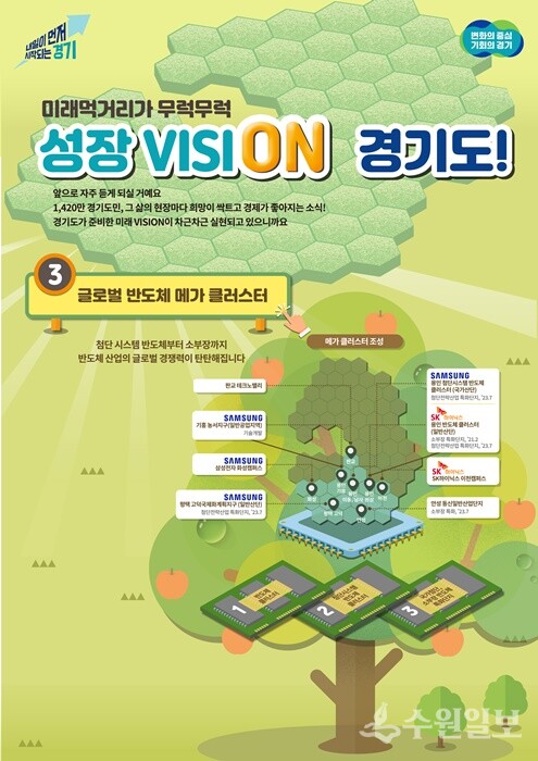
[Suwon Ilbo=Reporter Kim Gap-dong] Gyeonggi Province is drawing attention as it designs the future of the 'K-Semiconductor Industry' by establishing the 'world's largest semiconductor mega cluster' equipped with the entire semiconductor cycle from design to mass production, research, and talent development.
South Korea's domestic semiconductor industry ranks second globally with 18.5% of the world market share. The province is the heart of South Korea's semiconductor industry, accounting for 84.7% of added value and 76% of sales in the domestic semiconductor sector.
During the eighth popular election term, Gyeonggi Province is building the world's largest-scale semiconductor mega cluster connecting 'Seongnam~Suwon~Hwaseong~Yongin~Anseong~Pyeongtaek~Icheon' to protect South Korea's semiconductor industry competitiveness.
This project consolidates semiconductor industrial complexes scattered throughout southern Gyeonggi Province into one ecosystem encompassing large-scale semiconductor production, research, talent development, and materials, parts, and equipment (materials/parts/equipment) companies.
First, the core industrial complexes of the semiconductor mega cluster are the Yongin Idong and Namsa (7.28 million square meters, 360 trillion won) and Pyeongtaek Goduck (3.9 million square meters, 120 trillion won) semiconductor clusters being developed by Samsung Electronics, as well as the Yongin Wonsam (4.15 million square meters, 122 trillion won) semiconductor cluster being developed by SK Hynix. Approximately 600 trillion won in private investment is planned through 2047, and upon completion, it is projected to become the world's largest semiconductor production complex.
Shortly after the government designated the Yongin Idong and Namsa areas as a candidate national industrial park in 2023, the province formed a dedicated semiconductor support task force to provide rapid administrative support, including consultations with cities and counties, listening to residents' opinions, and resolving corporate challenges.
Through these efforts, Samsung's Advanced System Semiconductor Cluster National Industrial Park shortened the industrial park planning approval period, which typically takes four years, to one year and nine months. Starting with land compensation in the second half of this year, the province aims to begin industrial park construction in the second half of next year and complete the project in 2031.
Samsung Electronics plans to operate its first semiconductor fab in late 2030. SK Hynix's Semiconductor Cluster General Industrial Park has also mostly completed land and fixture compensation and is progressing smoothly with a project completion rate of 70.5%.
In Pangyo (fabless cluster), Suwon (R&D Park), Icheon (manufacturing, SK Hynix), and Anseong (materials/parts/equipment special zone), design and research facilities, production, materials, parts, equipment, and talent development institutions linked to Yongin and Pyeongtaek are gradually establishing themselves.
The province is building a 'Pangyo Fabless Cluster' by attracting fabless companies and support facilities to the Third Pangyo Techno Valley. Here, it plans to focus on developing and operating fabless company support programs in connection with the existing First and Second Pangyo Techno Valley.
In September of last year, the province established a System Semiconductor Development Support Center in the Second Pangyo Techno Valley to enable fabless companies to utilize advanced technical equipment and specialized personnel. On the 7th of this month, the province opened the 'Gyeonggi Province Fabless Academy' in the First Pangyo Techno Valley and plans to foster semiconductor design specialists through customized education tailored to fabless companies' workforce needs.
In July of last year, the 'Gyeonggi Province Semiconductor Technology Center' opened at the Next-Generation Convergence Technology Research Institute within Gwanggyo Techno Valley in Suwon to handle semiconductor new product development, technology verification, and professional personnel development. Composed of a performance test facility (testbed) for semiconductor materials, parts, and equipment technologies and a semiconductor workforce development center (G-SPEC), it strengthens support for small and medium-sized enterprises' prototype manufacturing and technology verification and plays a role in nurturing practical on-site specialists responsive to corporate needs.
In Anseong, the Dongshin General Industrial Park was designated on July 23, 2023, covering 1.57 million square meters in Dongshin-ri and surrounding areas in Bogae-myeon, Anseong-si, as a materials, parts, and equipment special zone. The industrial park plan approval application was submitted in June of this year, and administrative procedures are underway, with completion and corporate relocation planned by the end of 2030.
Global semiconductor companies are also establishing themselves in Gyeonggi Province, accelerating ecosystem construction.
The province succeeded in attracting production facilities and research and development (R&D) centers of the world's four major semiconductor equipment companies: America's Applied Materials (AMAT), the Netherlands' ASML, America's Lam Research, and Japan's Tokyo Electron (TEL).
ASML, the world's largest semiconductor lithography equipment company, has established an advanced extreme ultraviolet (EUV) cluster in Dongtae, Hwaseong, and semiconductor and display equipment company AMAT is also pursuing the establishment of a next-generation R&D center in Osan. Tokyo Electron completed and began full operations of its research and development center in Hwaseong. America's Lam Research Korea Technology Center moved into Jigok General Industrial Complex in Yongin, and the company has a semiconductor manufacturing plant in Osan and semiconductor sales and distribution facilities in Seongnam.
Governor Kim Dong-yeon stated, "Gyeonggi Province's 'K-Semiconductor Mega Cluster' strategy is a project that drives South Korea's future as the 'center of the global semiconductor industry' beyond the domestic market," and added, "All-around efforts are underway in investment attraction, talent development, technology infrastructure construction, and new industry linkage, which will become a core asset affecting the global competitiveness of Korean semiconductors."